I2S to TDA1540 converter Tutorial
Tutorial How to programm I2S converter Altera CPLD for DAC TDA1540
This device is converting standard I2S data (64fs) to the offset-binary data needed for TDA1540 DAC.
- "I2S 2x32=64-bit = 64fs" to "14-bit offset-binary" with inverted MSB and inverted stop-clocked BCK) for TDA1540 DAC (stereo) without the use of MCLK (= even less digital work)
- basic data synchronisation is incorporated on LRCK signal
- the sound is nice, very musical, clean, without digital interference
- my VHDL code is very simple, without advanced techniques, based mostly on standard logic
- therefore inexperienced users can understand and modify it for other similar DACs
- it has low load on the CPLD and it takes up little memory
- only 3 signal wires (I2S) are needed for input (DATA, BCK, LRCK).
- output is true offset-binary specified for TDA1540:
-- CL - stopped Left DAC clock
-- DL - Left DAC data (inverted MSB)
-- CR - stopped Right DAC clock
-- DR - Right DAC data (inverted MSB)
-- LL and LR - Latch for both channels (latched together)
- it flawlessly works with the cheap CPLD EPM240T100C5 from aliexpress and can be easily configured for others
- my VHDL code is open and free for all
If you like my work and find it helpful, you can donate coffee for me 😍
Donate Coffee for miro1360 Thank you 😊
----------------------------------------------------------------------------------------
What do you need:
- Altera CPLD MAX II EPM240T100C5N
- Altera programmer (USB Blaster)
You can buy both on aliexpress very cheap: click
- DC power supply (+5V from DAC PSU, or can be anything up to +12V ... or you can use +9V battery for this programming)
- Project files: download (download the whole rar file - download button in top right corner)
- Quartus Lite Software (free version, follow tutorial steps)
- Windows PC
Steps:
1. Search with google: Intel® Quartus® Prime Lite Edition Design Software and open the official Intel download website (normally the first link)
2. Select the latest version
3. Select individual files
4. Click on Download QuartusLiteSetup and save the file

5. On the website under Devices download the Intel® MAX® II, Intel® MAX® V Device Support file, create a new folder (like C:\Intel_Devices) and save it here

6. Install the Quartus Lite (simple setup - next, next, accept, next ...) and Finish the installation

7. Continue with automatic driver installation (next, install, finish) (if you uncheck the Launch USB Blaster II installation in the previous step, then this step does not appear ... we are using an older USB Blaster and another driver will be installed later)
8. Run the Quartus Lite
9. Click Yes, Next

10. Select the folder with downloaded Devices file and click Next

11. Select all components and click Next, Next, Finish and restart the Quartus Lite

12. Close Quartus Lite
13. Connect Altera programmer device with the CPLD board
14. Connect a power supply to the CPLD board and turn on the CPLD board with ON-OFF button (red LED turns on) ... the PSU can be connected either on +5V pin and GND pin on the CPLD board -- it can be the voltage from DAC PCB, or alternatively it can be connected in the black power supply connector (this DC voltage can be higher, like from a router adapter or +9V battery, I recommend not more than +12Vdc). This voltage is mandatory not only for programming, but also for the device operation.
15. Insert Altera programmer into USB port
16. Right click This Computer - Management - Device Manager and under Others you will see USB-Blaster (driver is not installed)
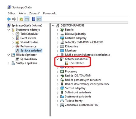
17. Right click USB-Blaster - Driver Update - Search driver in this Computer
18. Click Search and navigate C: - intelFPGA_lite - xxVersion - quartus - drivers - select usb-blaster folder and click OK
19. Click Next and wait for driver installation, then click Close and also close Device manager
20. Create a new project folder (like C:\Quartus_Projects)
21. Unpack the project file in this folder


22. Open Quartus Lite
23. In the Quartus Lite click File - Open Project, navigate into the project folder and select the project file and click Open (If it ask you something click Yes, Yes)

24. In the Quartus Lite click Tools - Programmer and the Programmer window will be open
25. Click Hardware Setup
26. For Currently selected hardware: select USB-Blaster and click Close

27. The USB-Blaster is now selected in the Programmer window
28. Click all checkboxes under Erase and click Start


29. Uncheck boxes under the Erase and check all boxes under the Program/Configure (you can also add all boxes under the Verify) and click Start

30. Close all and disconnect the CPLD from programmer device.
Now your CPLD is programmed and ready for the connection with DAC.
For further programming you just skip the installation steps.
If you struggle with drivers installation: #11494
Pins diagram
I2S - CPLD converter:GND with CPLD GND (next to the pin 21)
CPLD converter - DAC:
psu +5V with CPLD +5V pin (next to the pin 56 or the black power connector) ... or alternatively a higher voltage (max. +12Vdc)
All data pins can be reconfigured in the Quartus Lite (Assigments - Pin Planner) ... I don't recommend you do it, unless you know what you do.
Wiring all together:

Great tutorial, i will surely give it a try. Only question I have is how to USB to I2S converter works. How and to what do you hook the usb side of the converter up. What software do you need to run?
ReplyDelete